
 USA
USA Belgium
 France
 UK
UK Australia
 India
India Singapore
Innova Solutions: Leading the Semiconductor Revolution
May 25, 2023
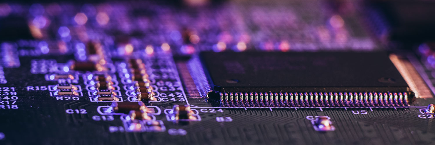
The Importance of Semiconductor Technology
Semiconductors are indispensable to modern society. These hardware components are integral for the functioning of computers, smartphones, medical equipment, and even simple switching circuits. As semiconductor technology advances, new devices and opportunities will arise across a wide range of industries. A combination of semiconductors and powerful software can allow us to explore new applications that will benefit people all over the world by combining artificial intelligence and machine learning. A breakthrough in semiconductor technology has the potential to profoundly impact the future of mankind. To achieve excellence in semiconductor technology, professionals must continue to research new technologies that will push the limits of our devices’ capabilities.
Innova Solutions’ Role in Semiconductor Technology
In the age of the Internet of Things (IoT), analytics, machine learning, and more, data is growing and becoming more complex; semiconductors are the engines driving it all. Innova’s team understands that fundamental SoC design paradigms must change to deliver more data, at faster speeds and with lower power and latency. The ability to fit more transistors onto ever smaller chips is limited as we reach the reticle ceiling of manufacturing. To achieve such performance gains, semiconductor innovation must be overhauled, and Innova is driving this transformation.
Using us as your preferred ASIC vendor, all you must do is provide us with the front end of your design and wait for the chips to arrive. Innova Solutions utilizes cutting-edge technologies, such as FPGAs, to provide innovative and effective solutions. FPGAs (field-programmable logic boards) are integrated circuits (ICs) capable of being programmed and reprogrammed by a user. FPGAs are classified as field-programmable because their capabilities are adjustable, as opposed to being hard-wired by the manufacturer as is the case with other ICs. FPGA technology can be modified after manufacture based on adaptive hardware to provide fundamental functionality. As a result, it is possible to construct highly efficient, domain-specific architectures using arrays of configurable hardware blocks.
Verification, Validation, and the Testing Process
In areas like artificial intelligence, the speed of innovation makes FPGAs more necessary than ever before. During the manufacturing process, you need to ask a few essential questions:
- Can you verify that a feature has been tested?
- How will it be validated?
- Which design defects have you discovered; how will they be corrected?
Innova Solutions prides itself on the rigorous Verification, Validation, and Testing process we employ to make sure that the product is error-free and that you, as the consumer, are satisfied. Laboratory testing is conducted on the manufactured design (chip) as part of our SoC Validation process. Along with the chip, all other components of the system are constructed on test boards or reference boards. Our aim in the design qualification process is to validate all possible uses for the chip that the customer might experience in practice. To ensure the reliability of SoCs and to ensure proper electrical characterization, they are screened for faults, random defects, reliability, functional defects, and reliability. Functional test patterns are used to identify functional defects. Identifying functional test patterns is the key to testing a chip at real speeds and achieving satisfactory coverage. A good quality chip can be harmed by errors in more than just financial terms, so we implement a methodology called Design for Testability (DFT). This methodology adds several features to test the chip, which results in a significant reduction in errors.
Pre-silicon and Post-silicon Validation
For silicon products, there are two distinct validation phases: pre-silicon and post-silicon validation. Virtual environments, such as simulators or emulators, are used for pre-silicon testing. As opposed to post-silicon validation, pre-silicon validation uses real-world scenarios. Performing pre-silicon validation is an essential first step in developing and testing products because it ensures that the SoC will have a basic level of operational functionality even before silicon is fabricated.
Performing post-silicon validation is one of the largest, most complex, and costliest parts of SoC design. Using various tests and software, our examiners keep track of the SoC and verify it works under actual conditions. Innova is dedicated to fostering the development of a common framework so that software developers can easily port their applications from one device to another, move software from one device to another, and enable easy device testing to create economies of scale.
Innova Solutions’ Services
Innova has extensive experience providing IT solutions and streamlining the management of product life cycles for semiconductor companies—from conceptualizing and connecting devices to developing embedded software and hardware for various industries. The company’s expertise in this area includes connectivity protocols, such as BLE, Zigbee®, Z-Wave, NBIoT, LoRa, Thread, NFC, MQTT, Ethernet, Wi-Fi, 2G/3G/4G/5G, and Wireless Mesh Technology. From silicon to firmware to host software, drivers, board design, and system testing, Innova’s customized tools and products can accelerate time to market, saving clients significant time and money.
About Innova
Founded in 1998 and headquartered in Atlanta, Georgia, Innova Solutions employs approximately 50,000 professionals worldwide and reports an annual revenue approaching $3 billion. The company’s robust offerings span across an array of industries and include Digital Product Engineering; Customer Experience; Cloud Services; Data & Insights; Intelligent Automation (AI); Cyber Security; Managed Service Provider (MSP) Services; Talent Solutions; Direct Sourcing; and Business Process Outsourcing. Through global delivery centers across North America, Asia, and Europe, Innova delivers strategic technology and business transformation solutions to clients, enabling them to operate as leaders within their fields.